APPLICATIONS

Applications

Real measurement results showing 3D imaging modules in advanced packaging and precision-electronics inspection.

VERIFIED RESULTS

From inspection challenges to measurement evidence

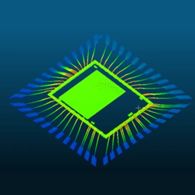
3D measurement result for micro-assembly module

PSR2000 Series

Micro-assembly module inspection

Capture clear images of reflective dies and first/second bond points while measuring aluminium-wire arc height and die glue height.

Industry
Advanced semiconductor packaging / micro-assembly
Inspection scope
3D height measurement, 2D grayscale imaging, wire and dispensing process inspection
View full case
Lead-frame and high-speed optical module inspection inspection result

PSR2000 Series

Lead-frame and high-speed optical module inspection

Synchronously present 3D height and 2D grayscale results for lead-frame CMOS sensors and 800G optical-module optoelectronic chips.

Industry
Lead frames / high-speed optical communication modules
Inspection scope
Die warpage, placement offset and surface topography defect inspection
View full case
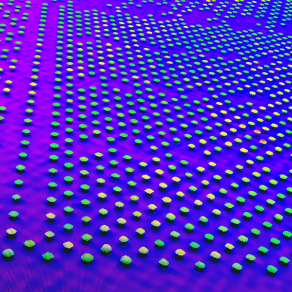
3D measurement result for micro solder-paste height

PSR2000 Series

3D Inspection of Micro-Bumps

Designed for advanced packaging applications such as CoWoS, this solution performs 3D topography and cross-sectional profile measurement of microbumps on wafer surfaces, delivering synchronized 3D height and 2D grayscale outputs.

Industry
Advanced Semiconductor Packaging / CoWoS
Inspection scope
Measurement of microbump height, diameter, coplanarity, and 3D topography
View full case
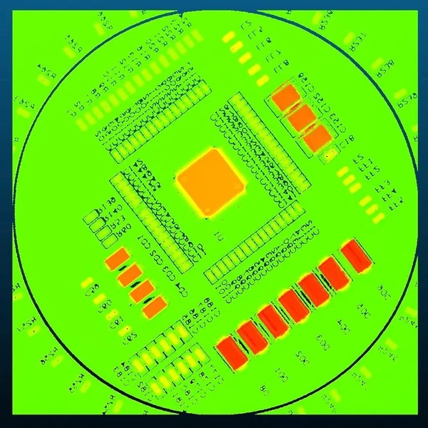
PCBA and BGA inspection inspection result

PSR1000 Series

PCBA and BGA inspection

Inspect PCBA chips, resistors, capacitors and BGA solder balls with 3D maps, 2D height maps and profile sections.

Industry
Precision electronic structures / semiconductor packaging
Inspection scope
PCBA component geometry, BGA array and height-profile inspection
View full case