
BACKGROUND
Project background
Optical communication chip placement and lead-frame structures demand high placement accuracy and consistent surface geometry.
PSR2000 Series / CASE 202
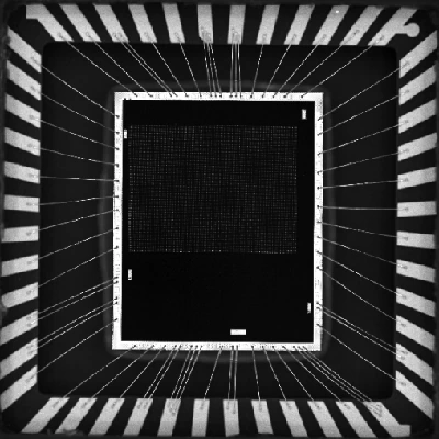
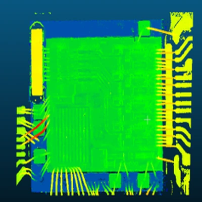
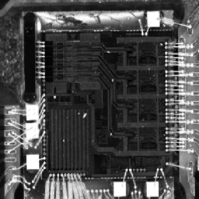
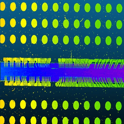
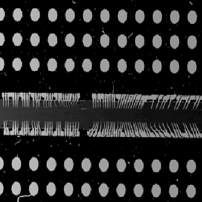
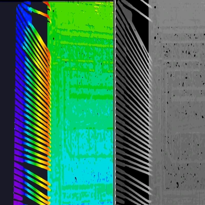
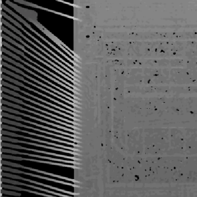
Synchronously present 3D height and 2D grayscale results for lead-frame CMOS sensors and 800G optical-module optoelectronic chips.
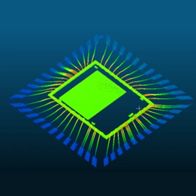
BACKGROUND
Optical communication chip placement and lead-frame structures demand high placement accuracy and consistent surface geometry.
CHALLENGE
The inspection must judge die warpage, placement offset and surface defects across reflective chips and complex lead structures.
SOLUTION
PSR2000 combines reflective-part measurement with synchronized 3D + 2D output to provide height and grayscale evidence in one field of view.
RESULTS
MEASUREMENT EVIDENCE
DISCUSS YOUR SAMPLE